Impedance of Laser DiodesInductive behaviour
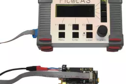
Related Products: LDP-AV, LDP-V, LDP-CL
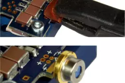
The parasitic stray inductive behaviour is the most important influence on the pulse rise time. The output voltage of the driver must be able to charge the stray inductance, thus resulting in slower current rise times. The following table shows the stray inductance of commonly used laser diode packages.
Package drawing
Package style
Package inductance
1
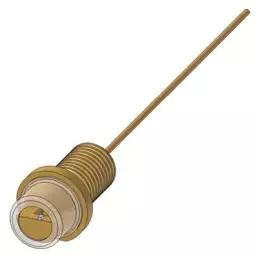
Source: LASER COMPONENTS GmbH
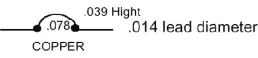
8-32 coaxial
12 nH*
2
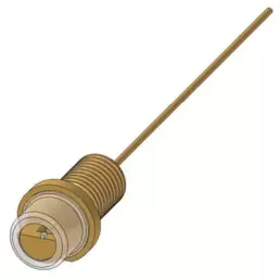
Source: LASER COMPONENTS GmbH
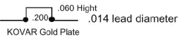
10-32 coaxial
11 nH*
3
Source: LASER COMPONENTS GmbH
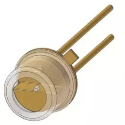
TO-5 2-lead
9,6 nH*
4
Source: LASER COMPONENTS GmbH
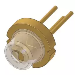
TO-52
5,6 .. 6,8 nH*
5
Source: LASER COMPONENTS GmbH
CD 9mm
5,2 … 6,8 nH*
6
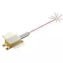
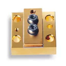
Butterfly
22 nH**
7
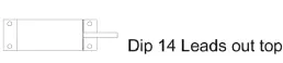
Dip 14 leaded
15,7 nH
8
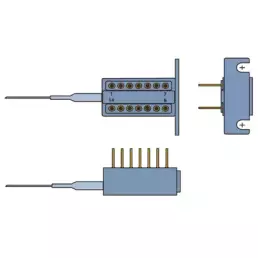
Long Horn 14 Pin
6,4 nH**
9
Source: Bookham
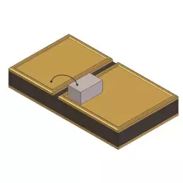
Maxi-Chip and similar
2,6 nH**
10
Source: LASER COMPONENTS GmbH
Y-Package
1,6 nH*
11
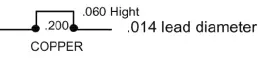
Lead-loop
5,0 nH***
12
Lead-loop
3,6 nH***
13
Lead-loop
1,56 nH***
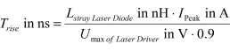
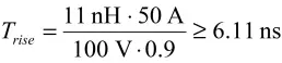
With a known stray inductance the fastest possible rise time can be roughly estimated with the following Rule of thumb:
E.g. using a LDP-V 50-100 and a „10-32 coaxial” (#2):
* Manufacturers values. Refer to www.lasercomponents.com for detailed information and package drawings
** Measured values
*** Calculated values